LC3 Machine Instruction
08 Jun 2020In order to supplement our understanding of LC3 datapath, here we introduce Machine Instruciton in broad stroke to learn how data move along the datapath.
Machine Instruciton are 16-bit lowest level instruction that LC3 CPU can understand.
There are 3 categories of machine instructions–Operation, Data Movement, and Control:
Operation (ALU)
Data Movement (MEMORY)
Load–bring data from external memory into the CPU
Store–takes value from one of the 8 registers and save it to the memory address
Control
Conditionals
Loops & Functions (Subroutines)
OP Code and Instructions
Figure 1 shows some Machine Instructions and the bit-allocations for their 16 bits
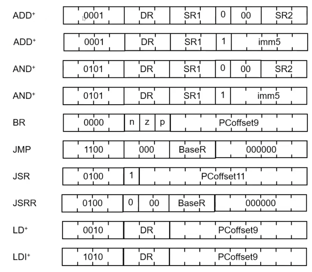
For example of the first ADD+, 0001is ADD’s OP code, which stands for Operation Code. DR is the Destination Register, which is stores address of the output. SR1is the Source Register 1, which holds the first operand. SR2is the Source Register 2, which holds the second operand.
In assembly language, we would write ADD R2, R1, R3, which means add R1 and R3, and store the result in R2. On a high level langauge, it can be translated as R2 = R1 + R3.
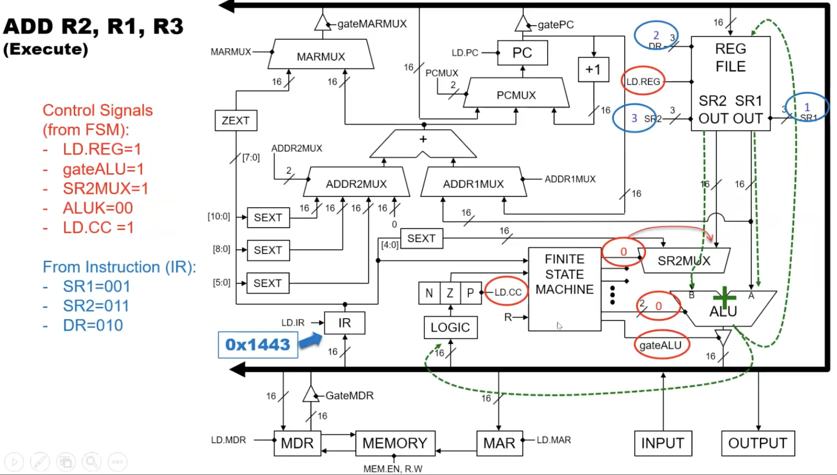
Closer Look at ADD
FSM turns on specific control signals in LC3, which activates certain paths in the datapath. The signals specify how data moves in the datapath to be used in operations like addition. The FSM fetches and decodes each instruction before executing the operation.
Tracing the ADD example
Fetch
Fetch takes 3 clock cycles (3 consecutive states) to read data from memory.
The ADD machine code instruction lives as a 16-bit memory in Instruction Register (IR) in consequtieve sequence with other instrcutions of the same program. The Program Counter (PR) stores the memory address of the next instruction to be executed.
Before the ADD instruction can be executed, in the first fetch clock cycle (state 18), the PC has to indicate the memory address of where the instruciton is located.
The output of PC then passes through the 1-bit Tri-State Buffer and gets onto the bus, which then sends the data into Memory Address Register (MAR). LD.MAR–the WE of MAR–turns on to receive the data. and PC increments to the next line of the program.
The 2-bit PCMUX selector selects one of the three choices to pass address data from PCMUX into PC: adder to increment the PC (+1), data from bus to PC, and data from effective address calculator to PC. The 1-bit PC WE–LD.PC–turns on to read in the output from MUX. In the case of ADD, PC becomes PC*, where PC* = PC++.
The reason why the PC can simulataneously output its current value as it reads in the self-incrementing instruction is because of the Leader-Follower Flip Flop.
In the second fetch clock cycle (state 28), the data is read from MAR into the big Memory, and then from big Memory into the Data Register (MDR). FSM turns on MEM.EN and LD.MDR–the WE in both big Memory and MDR–respectively.
In the third fetch clock cycle (state 30), the data flows from the MDR into the IR. To do so, data first passes through the Tri-State Buffer gateMDR onto the bus. IR’s WE LD.IR is turned on by the FSM and pays attention to the data on the bus and receives it into IR.
This program takes 4 bits of control signal total from the FSM.
Decode
Decode (state 32) is where the FSM generates the control signals for the specific instruction, which is ADD in this case; it takes 1 clock cycle.
Execute
Nnow we have the values from R1 and R3 (as fetched from IR), and we want to perform addition and store data in R2 next.
The steps happen in sequence:
1. SR1 reads data living in Reg1001and flow the data to ALU 2. ALU input is already listening for input from SR1 at input A 3. SR2 reads the data living in Reg30114. Data in SR2 goes first into the SR2MUX. Selector input, set to 0, will select the data from SR2 5. The ALU 2-bit selector selects the number that represents ADD (in the case of LC3, ADD =00) 6. ALU performs combinational logic of addition of the two numbers 7. ALU outputs the result of ADD 8. Tristate Buffer gateALU sets to 1, giving green light for ALU to send data to the bus 9. Everyone on the bus except for Reg File and NZP Reg ignore the number 10. Reg File turns on its WE--LD.Reg--so it can receive the data output from ALU as its input 11. NZP Reg turns on its WE--LD.CC. NZP listens whenever ALU does math so it knows properties of the output
ADD only takes 1 clock cycle in the execute phase of machine instruction. But in general, the number of cycles taken in the execute phase depends on the instruction. After the execution phase, the FSM returns to the first fetch state of incrementing and transporting the PC onto bus.
Figure shows the ADD execute phase of machine instruction.
LC3 is a FSM
The LC3 has 64 possible states.
…and orchestrates 42 control signals, including:
- Multiplexer Selectors
- PCMUX
- MARMUX
- ADDR2MUX ...
- Tri-State Buffers enable
- gatePC
- gateMARMUX
- gateALU ...
- Register WE
- LD.PC
- LD.REG
- LD.MAR
- LD.CC ...
- Other control signals
- ALUK (which selects the ALU operation to perform)
- MEM.EN
- R.W ...